RAVE TO THE GRAVE
Table of Contents
This manual describes version 1 of the RAVE TO THE GRAVE.
Features
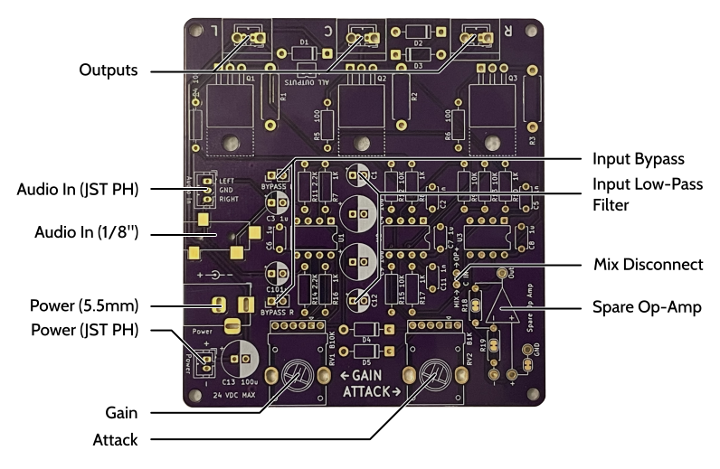
Power comes through either a 5.5mm barrel jack (center positive), or a JST PH connector. The maximum input voltage is 24V. The minimum voltage is probably around 4-5V due to the MOSFET gate thresholds, the high-side headroom the LM358 needs, and the voltage you need to light up your outputs.
Audio input can come from either a 3-pin JST PH connector or a 1/8" stereo phono jack. It expects line-level input, though it is not too picky as the gain knob can adjust this from about -7dB to +7dB (if I'm doing my math correctly).
The gain knob adjusts the audio sensitivity, and increasing it will drive more current through the outputs. The attack knob controls how quickly the C4 and C9 capacitors get charged by the audio level, which controls the "smoothness" of the audio level response.
The Input Bypass, Low-Pass Filter, Mix Disconnect, and Spare Op-Amp are described in the Build and Configuration section.
Theory of Operation
The RAVE TO THE GRAVE is a fairly standard peak level detection circuit followed by a linear constant-current sink. Each of the left and right channels are an independent copy of this. Let's look at the left channel.
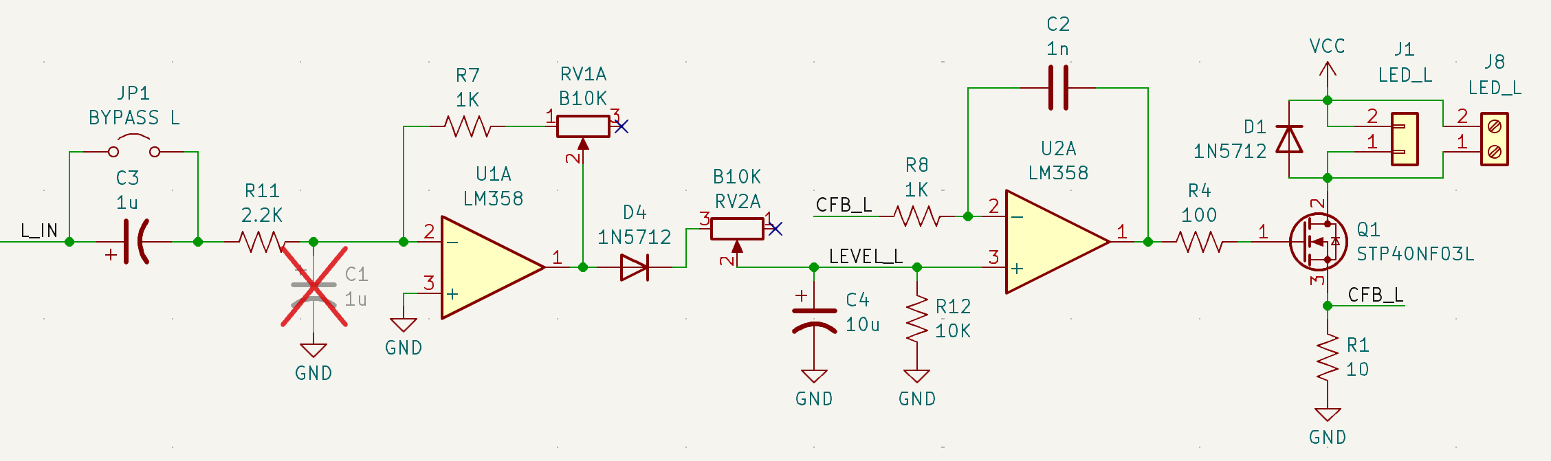
Audio comes in through C3, which blocks the DC offset of the input signal. Next the signal passes throug the inverting amplifier formed by R11, R7, RV1, and U1. RV1 adjusts the amplitude gain of this amplifier from 0.45 to 5.
The output of this amplifier is rectified by D4, which captures the peak level of the signal in C4 after passing through RV2. RV2 controls the amount of current entering C4, which controls the attack. R12 discharges C4.
The voltage level on C4 is one input of the current control loop formed by R8, C2, U2, R4, Q1, and R1. The op-amp continuously compares the voltage across R1 against the voltage across C4 and adjusts its output to control the gate of Q1. Because R1 is connected to the source of Q1, it measures the current through Q1, so the op-amp is controlling the current flow through Q1. Thus, the audio peak level captured on C4 creates a proportional current through Q1, driving the load proportionally to the amplitude of the audio input.
The center channel is just a third constant-current driver circuit fed from a 50/50 mix of the left and right channels.
Build and Configuration
The input audio connectors are directly connected together. They cannot be used simultaneously. Likewise, the input power connectors are directly connected. Use only one of them.
If the audio level is referenced to the same ground as this board, the BYPASS L/R jumpers can be used and C3 and C10 can be omitted.
The caps C1 and C12 should be omitted unless you want to low-pass filter the output. This might be useful if you want to detect only the low-frequency bass drum. The 2.2kΩ resistor should not be replaced with a lower value as it is important to prevent current overloads due to negative voltage excursions on the input signal. Changing it will also affect the amplification factor of U1. The exact cutoff frequency of a 1uF capacitor is left as an exercise to the reader. :)
There is a unused op-amp on U3 that is broken out for your experimentation. It is configured as a unity gain amplifier with the input tied to ground, but you can cut the jumpers to reconfigure it however you like.
The C IN jumper is connected by default and connects the L/R mix to the center channel op-amp and driver. This connection can be cut and some other signal can be connected to it if you wish.
The output footprints support both JST PH and 5mm screw terminal blocks. Note the polarity on the silkscreen. You can use a separate higher voltage to power the loads so long as it shares the same ground. This voltage is limited only by your MOSFETs.
The output diodes D1, D2, and D3 are optional depending on your load. For driving LEDs, they are probably unnecessary, but if you want to drive something inductive (like a light bulb or a motor), you should install them.
I've used STP40NF03L MOSFETs in the schematic but that's just what I had on hand and you do not need any specific kind of power MOSFET to make this work. Probably anything you can find in a TO-220 form factor these days will work, though you should mind that their gate threshold voltage works for your input voltage as the LM358 can only output at best ~1.5V below the positive rail.
The MOSFETs are intended to be mounted face down, with the metal tab facing up. For light loads they are probably fine like that, but otherwise a small heatsink should be fitted as they are going to be constantly in the linear region. With a thin heatsink, a M3x10 screw fits through with just enough space for a nut on the other side. I spaced them to fit the Wakefield 289-AB heatsink which is about 1 inch (25.4mm) wide, but there is about 4 mm margin between them so other heatsinks should fit as well.
The load sensing resistors R1, R2, and R3 are a limiting factor for maximum load current. With 1W resistors you can safely drive up to 100mA, and 2W gets you 200mA. You can decrease the value of these resistors to increase the amount of current through these drivers. But watch the power dissipation across the MOSFETs. Especially at higher voltages, they will be dissipating a lot of heat at higher currents. For example, if you use 2.2Ω 2W resistors, you can sink 950mA before the resistors are toast, but at just 12V the MOSFET will be dissipating 9.4W. And there are three of them! You will want to think about active cooling if you go down this road.
I suppose you could use different op-amps if you wanted. Being able to drive close to the positive rail might help depending on your choice of MOSFET, but I don't think there's much other reason to use anything better than the LM358.