SQWAK BOX
Table of Contents
This manual describes version 2 of the SQWAK BOX.
Overview
The SQWAK BOX is built from three parts - the ATtiny24/44/84A microcontroller, a 25-series SPI flash ROM, and an LM4871 (or equivalent) audio amplifier. As designed, it plays a sound sample when an input is triggered.
Operation
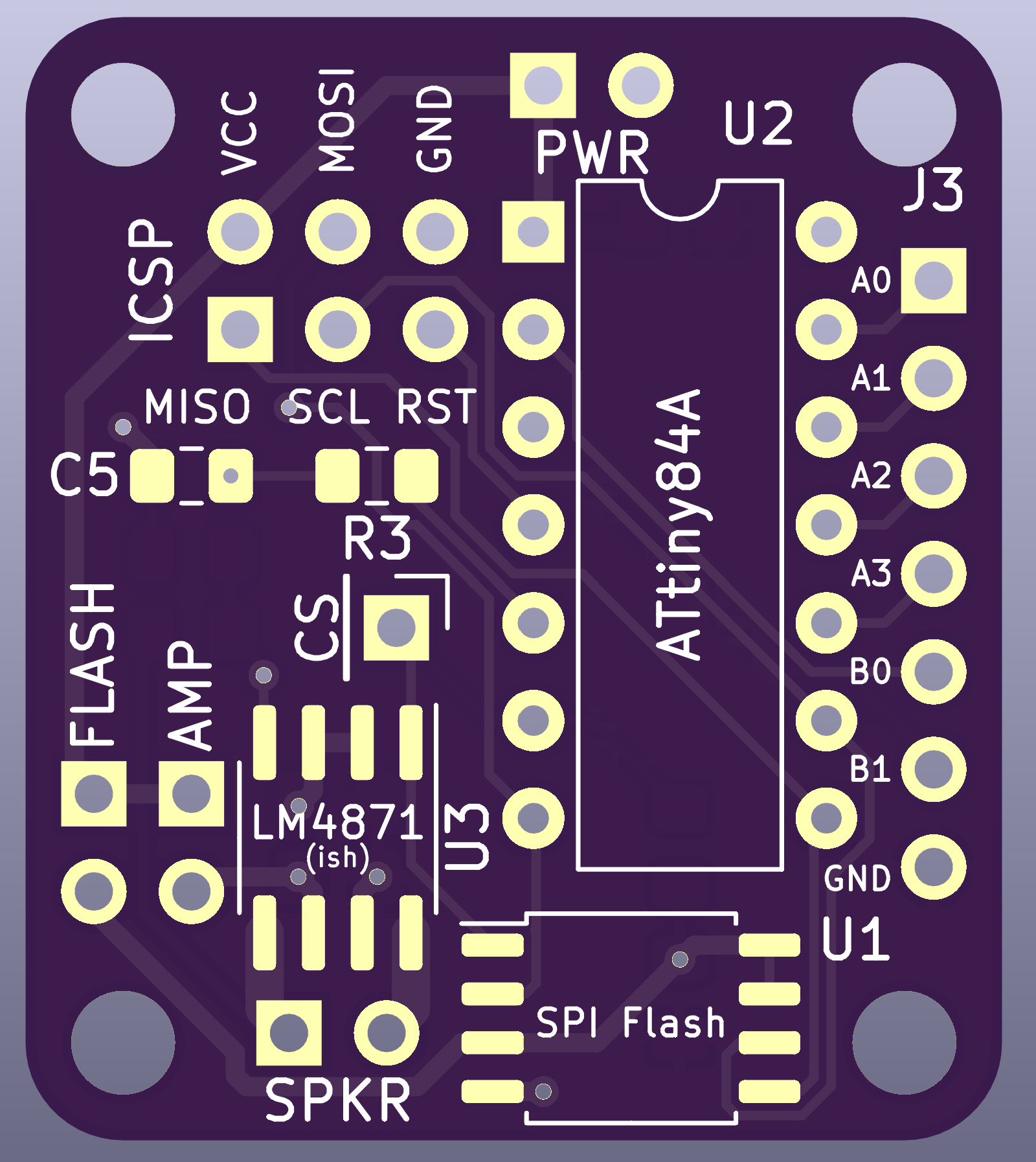
At the top are two power inputs, positive on the left, negative on the right. The board is designed for 3.3V, which is a limitation of commonly available SPI flash chips.
Moving downward, to the left of the ATtiny is a six pin AVR ICSP header, used to program the ATtiny in situ. Below this, floating in the middle of the board is the flash chip's CS pin, which is needed to program it in situ. To the left of the LM4871 is two jumpers which disconnect power to the amplifier and the flash chip (so that they don't interfere with programming the ATtiny). And at the bottom is the speaker output. A 4- or 8Ω speaker will work fine. There is no volume control.
Pins A0-A3, B0, and B1 are broken out for inputs, and by default sound is triggered by pulling B0 to ground. You can of course program them to do whatever you want, like an I2C line to another device.
The SQWAK BOX needs to be programmed. The software is available over here. Additionally, samples have to be converted and written to the SPI flash ROM, which is also described in the software repo.
The spacing of the PWR and A/B inputs are such that they can fit into a standard 830 position breadboard. This is useful for testing.
Assembly and Programming
Parts
The board was designed with the ATtiny84A, but the firmware easily fits on the smaller 24 or 44A. Sadly, any of these are pretty expensive nowadays, so this board is not as simple and cheap as it used to be!
The LM4871 has cheaper clones like the TC8002. They might sound a little worse but the LM4871 never sounded great to begin with.
You can use any SPI flash (or other device) that supports the usual 0x03 24-bit sequential read command. Samples can be as large as the flash device.
Programming
When programming the ATtiny through the ICSP, you should disconnect the FLASH jumper to remove power from the SPI flash. Otherwise the SPI flash will respond to the SPI programming commands and make a hash of it.
Likewise, when programming the SPI flash, you should disconnect the FLASH jumper and input power to the lower pin of the FLASH jumper, which powers the SPI flash directly. The ICSP pins are used for programming both.